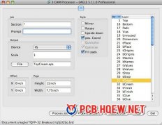
Manufacturing the USB PCB
You can achieve a really nice "DIY" feel if you etch the PCB yourself, but I choose to go for a "professional" look by sending my PCB design to a PCB manufacture. Please be aware of the file that your bitmap layer goes into! If you select the bitmap layer in the copper gerber file, then the bitmap w...
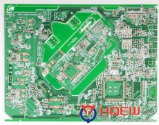
USB PCB Layout
Layout the component as shown, or you can be creative, as long as your layout matches the circuit. For low speed USB, you don't have to worry too much about how the traces are layed out. For high speed designs, you should try to keep the differential D+ and D- signals together and away from noise, bu...
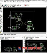
Turn Your Schematic into a PCB(Step 14 to step 19)
Step 14: Neaten up: smash package text If we want the names of components to be legible on the top of the board (transferred via toner transfer), or just to look good on printouts, they names and values probably have to be moved from their default locations. In order to move the text separately from...
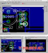
Turn Your Schematic into a PCB(Step7 to step13)
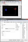
Step 7: Check signals to see how they'll route One way to get hints on part placement is to look at some significant signals to see whether they have nice straight paths, or whether they zigzag all over the board. First use the RATSNEST icon/command to have EAGLE recompute the airwires. The way thin...
Turn Your Schematic into a PCB
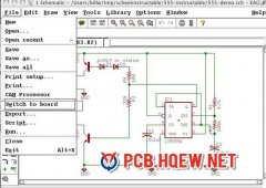
Step 1: Starting from the schematic... So this is the schematic we have from the Schematic Instructable. Up in the file menu, there's a "Switch to board" selection. If we do that from a bare schematic, it will offer to create the board from the schematic for us, and then leave us sitting in the Boar...

PCB Schematic Overview
Before you start drawing wires and stuff, you need to know what circuit you want to build. So you need to find or design schematics for your circuit. And you need a circuit design software. Then you are ready to begin the process. And that’s what we call PCB Schematic. here is a little guide that ...
Fibreglass Fighting Back As a PCB Substrate
It says something for the status of FR4 as an everyday material that people notice when a printed circuit board (PCB) is not green. Yet both the fibreglass – yet another product of silicon – and the UL94V0-rated flame-retardant resin that binds the fibres together – the source of the FR in FR4 –...
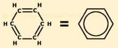
Basic Aromatic Structure
The structural formula for cyclic carbon compounds can be abbreviated by eliminating the carbons and hydrogens and using an inner ring to indicate that the double bonds continuously flip between the carbons. For simplicity sake, the abbreviated form of the aromatic rings will be used in this article....
PCB Manufacturing Process Evolution
Eventually processes were developed that would plate copper onto the walls of the drilled holes. That allowed circuits on both sides of the board to be connected electrically. Copper had replaced brass as the metal of choice because of its ability to carry electrical current, relatively low cost and ...
PCB Substrate Overview
Polychlorinated biphenyls commonly known as PCBs are man made chemicals that never existed in nature until the 1900's when they started to be released into the environment by manufacturing companies and consumers. First manufactured by Monsanto (the only American company to manufacture PCBs) in 1929,...