Extreme Copper Printed Circuit Boards
The special requirements for the design of Heavy Copper printed circuit boards, EXTREME Copper printed circuit boards and PowerLink printed circuit boards and other forms of component mounting and interconnecting structures incorporating copper weights ≤ 3oz/ft2. Some sections of this standard are ...
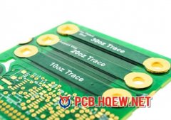
Heavy Copper Printed Circuit Boards
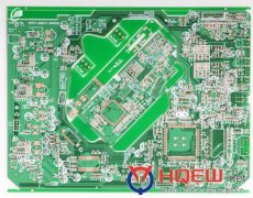
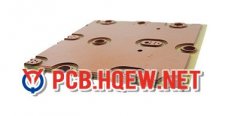
HQPCB has been building heavy copper circuit boards with traces and copper planes of up to 6 ounces for over 20 years. Our expertise is in producing at a reasonable cost, heavy copper PCB's that are of proven designs. Our engineering team can work with you to review your design to make sure that they...
Using Heavy Copper in PCB Design and Fabrication
An increasing number of power electronics products are taking advantage of a growing trend in the printed circuit board industry: Heavy Copper and EXTREME Copper Printed Circuit Boards. Most commercially available PCBs are manufactured for low-voltage/low power applications, with copper traces/plane...
Do's and Don'ts for PCB Layer Stack-up
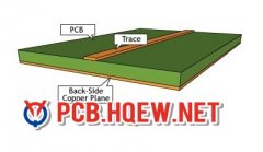
Do’s 1 As ground planes diminish the electromagnetic interference and electromagnetic radiation by absorbing high frequency noises, plan ground plane on the outer sides of the board. It is good practice to have ground plane on either one-side or both-side of board. 2 Noise and crosstalk generati...
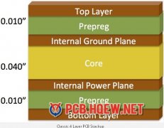
4 Layer PCB Stackup
The classic 4-layer PCB stackup includes two routing layers and two internal planes, one for ground and the other for power. Adhering to this stackup, including the core and prepreg heights shown, while utilizing FR-4 PCB materialand 1 oz copper, the properties of 50 Ohm traces on the routing layers...
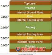
6 Layer PCB Stackup
The 6-layer PCB classic stackup includes four routing layers (two outer and two internal) and two internal planes (one for ground and the other for power). Again, adhering to this stackup while utilizing FR-4 PCB material and 1 oz copper, the properties of 50 Ohm traces are provided in the table bel...
How to Design PCB Stackup
There are two options: 1 Leave your PCB manufacturer to design PCB stackup for you You don’t need to spend your time by designing stackup. Leave it on PCB manufacturer – they are professionals. They do it every day. Also, by doing it this way, you can work on design in parallel of handling iss...
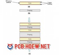
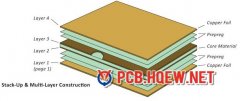
Layer Stack-up Basics
Layer stack-up specifies the proper arrangement of circuit board layers for multilayer boards before starting board layout design. Stack-up mainly defines which layers should be solid power and ground planes, the substrate (dielectric constant), and the spacing between layers. While planning a ...

How to Learn PCB Layout
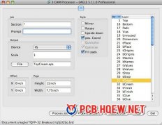
Instructions 1 Download and install the PCB design software of your choice. There is a wide range of PCB design software packages available, from high-end commercial products to freeware tools. Some offer a wider range of features than others, but they each function essentially the same way. 2 Ex...
Tools for PCB Design & Layout
ExpressPCB This is a free computer-aided design (CAD) software program designed for beginners or students. This program allows you to create schematic drawings via the ExpressSCH tool. You can use it to add components and pins, and connect these objects together via wires. A schematic drawing will h...